Gallium Arsenide (GaAs) Substrates
Gallium Arsenide (GaAs) Substrates
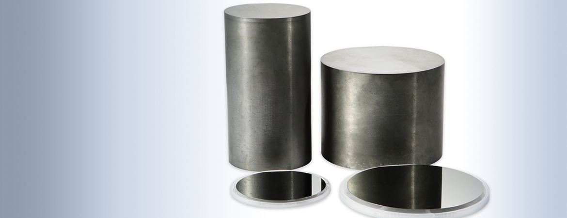
Vital Materials can provide up to 6-inch GaAs substrates grown with VGF technology, including semi-insulating GaAs wafers (without doping) and semi-conducting GaAs wafers (Si or Zn doped).
Market and Application
GaAs is a semi-conductor material with excellent performance characteristics including direct band gap, high electron mobility, high-frequency low noise, and high conversion efficiency.
The RF devices produced with GaAs substrates are commonly used in wireless communication applications, including wireless networks (WLAN), mobile communication, 4G/5G base stations, satellite communications, and WiFi communications.
With the development of mini-LED and micro-LED, red light LEDs produced with GaAs substrates are increasingly used for display screens and in AR/VR.
The conversion efficiency of a high-efficiency solar-cell panel based on GaAs is up to 40%. At present, such solar-cell panels are widely used in unmanned aerial vehicle and solar auto applications.
GaAs applications cover a large variety of transistors for industry spanning optical fiber communication, wireless networks (WLAN), mobile handsets, blue tooth communications, satellite communications, monolithic microwave integrated circuits (MMIC) for 5G, as well as radio frequency integrated circuits (RFIC).
With Vital’s extensive experience, we have established a strict quality control system that ensures the substrates achieve superior mechanical properties.
| Item | Unit | LD Applications Specifications | LED Applications | Microelectronics Specifications |
|---|---|---|---|---|
| Conduct Type | n-type | p-type/n-type | ||
| Crystal Growth Method | VGF | VGF | VGF | |
| Dopant | Si | Zn/Si | Undoped | |
| Diameter | inch | 2",3",4" and 6" | 2",3",4" and 6" | 2",3",4" and 6" |
| Wafer Orientation* | (100)±0.1° | (100)±0.5° | (100)±0.5° | |
| OF/IF | US or EJ | US or EJ | US, EJ or notch | |
| Carrier Concentration | /cm3 | (0.4-2.5) ×1018 | (0.5-5) ×1019 (0.4-4)×1018 |
|
| Resistivity (at RT) | ohm.cm | (1.2-9.9) ×10-3 | (1.2-9.9)×10-3 | >107 |
| Mobility | cm2/v.s | >1500 | 50-120/>1000 | >4000 |
| Etch Pit Density (EPD) | /cm2 | <500 | <5000 | <5000 |
| Laser Marking | Upon request | Upon request | Upon request | |
| Thickness* | μm | (350-650)±25 | (350-650)±25 | (350-650)±25 |
| TTV(P/P) | μm | ≤5 | ≤5 | ≤4 |
| TTV(P/E) | μm | ≤10 | ≤10 | ≤10 |
| Warp | μm | ≤10 | ≤10 | ≤10 |
| Surface | Side1 Side2 |
Polished Polished/Etched |
Polished Polished/Etched |
Polished Polished/Etched |
| Epi-ready | Yes | Yes | Yes | |
| Package | Cassette or single wafer container | Cassette or single wafer container | Cassette or single wafer container |