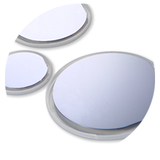
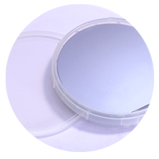
Wafer Substrates
Vital Materials is a manufacturer supplying gallium arsenide (GaAs), germanium (Ge) and indium phosphide (InP) substrates as well as related products. Vital Materials is one of the leaders in Chinese GaAs wafer market. We produce both semiconducting and semi-insulating GaAs and InP substrates. Electrical properties are customized based on customer requirements.
We control the conductive type (n and p type) and electrical property parameters of substrate crystals by adjusting the mix of elements and concentrations during the process of crystal growth. Standard doping elements include carbon (C), silicon (Si), iron (Fe), sulfur (S), zinc (Zn).
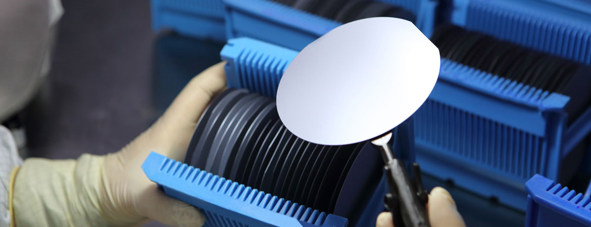
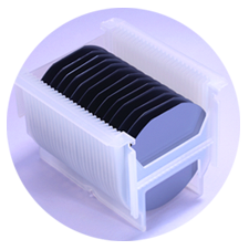
Vital Materials processes the substrate wafer to a highly uniform flatness with advanced high-precision wire-cutting equipment and high-flatness grinding and polishing equipment. CMP polishing process, cleaning process and packaging process provides for high-quality thin-film and epitaxial substrate wafers for epitaxy manufacturers.
We control the conductive type (n and p type) and electrical property parameters of substrate crystals by adjusting the mix of elements and concentrations during the process of crystal growth. Standard doping elements include carbon (C), silicon (Si), iron (Fe), sulfur (S), zinc (Zn).
Vital Materials processes the substrate wafer to a highly uniform flatness with advanced high-precision wire-cutting equipment and high-flatness grinding and polishing equipment. CMP polishing process, cleaning process and packaging process provides for high-quality thin-film and epitaxial substrate wafers for epitaxy manufacturers.
GaAs Wafers & Substrates
Vital Materials provides 2"-6" GaAs wafers including semi-insulating GaAs (un-doped), and semiconducting GaAs (Si-doped, Zn-doped).

InP Wafers & Substrates
Vital Materials provides 2", 3", 4" InP wafer, including un-doped InP wafer, Fe-doped InP wafer, S-doped InP wafer, and Zn-doped InP wafer.
Germanium Wafers & Substrates
Vital Materials provides 4" and 6" Germanium wafers, with a resistivity from 0.05 Ω·cm to over 50Ω·cm.